|
Product Details:
|
| Highlight: | ceramic vacuum chuck for machining,technical ceramic vacuum chuck,precision ceramic vacuum chuck |
||
|---|---|---|---|
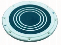
In advanced semiconductor, optical, and flat-panel display manufacturing, holding ultra-thin and fragile substrates without distortion or contamination is critical. Our Ceramic Vacuum Chucks are high-precision workholding systems engineered using porous or micro-channel advanced technical ceramics. By distributing vacuum pressure evenly across the entire contact area, they provide high holding force while preventing local strain, bowing, or surface scratching on delicate workpieces.
We offer two primary structural designs tailored to specific handling and processing requirements:
Porous Ceramic Vacuum Chucks: Manufactured with an interconnected micro-porous structure ($1 mutext{m} sim 10 mutext{m}$ pore size). Air is drawn uniformly across the entire ceramic surface, allowing for ultra-flat clamping of flexible films, thin wafers, and glass without leaving suction marks or localized pin-deformations.
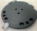
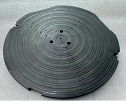
Pin-Type / Micro-Groove Ceramic Chucks: Features a dense ceramic body with precision-machined micro-pins or vacuum grooves. This design minimizes the contact area with the substrate, drastically reducing particle contamination on the back side of wafers.
Made from high-density ceramics such as Silicon Carbide ($SiC$) or Alumina ($Al_2O_3$), these chucks exhibit extremely low thermal expansion coefficients. They maintain flatnesses of $le 1 mutext{m}$ across large diameters even under elevated temperature processes.
Unlike traditional metal chucks that can mar, scratch, or transfer metallic ions to sensitive substrates, technical ceramics are non-contaminating, highly wear-resistant, and non-magnetic.
Impenetrable to chemical corrosion, making them ideal for spin-coating, wet etching, chemical mechanical planarization (CMP), and photoresist processing.
Available in conductive or semi-conductive ceramic grades to safely dissipate static charges during wafer loading, inspection, and unloading, preventing static damage to micro-electronic devices.
| Industry / Application | Specific Uses |
| Semiconductor Manufacturing | Wafer dicing, grinding, spin-coating, lithography, and inspection systems |
| Flat Panel Display (FPD) | Clamping OLED, micro-LED, and thin glass substrates during laser processing |
| Optics & Precision Metrology | Non-deforming holding of optical lenses, mirrors, and precision reticles |
| Flexible Electronics | Vacuum holding of ultra-thin films, foils, and flexible printed circuits (FPC) |
Contact Person: Daniel
Tel: 18003718225
Fax: 86-0371-6572-0196