|
Product Details:
|
| Highlight: | ceramic electrostatic chuck for high-vacuum,precision substrate clamping ESC,ceramic ESC for plasma environments |
||
|---|---|---|---|
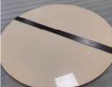
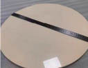
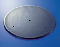
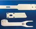
Ceramic Electrostatic Chuck (ESC) —— Precision Substrate Clamping for High-Vacuum & Plasma Environments
In advanced semiconductor fabrication and thin-film deposition, conventional mechanical or vacuum clamping methods fail to meet the ultra-clean, high-vacuum, and temperature-controlled requirements of sub-nanometer processing. Our Ceramic Electrostatic Chucks (ESC) utilize Coulombic or Johnsen-Rahbek (J-R) electrostatic forces to securely clamp wafers and substrates without mechanical edge contact, delivering exceptional temperature uniformity, wafer flatness, and particle reduction.
We engineer both primary electrostatic chuck configurations tailored to specific processing environments:
Johnsen-Rahbek (J-R) Type Ceramic ESC: Manufactured using semi-conductive ceramic formulations (such as doped Alumina or Silicon Carbide). Utilizing micro-leakage currents at the wafer-chuck interface, J-R chucks generate immense electrostatic clamping forces at lower operating voltages, making them ideal for high-density plasma etching and PVD/CVD processes.
Coulombic Type Ceramic ESC: Constructed with high-purity insulating ceramics. Clamping relies entirely on pure electrostatic charge accumulation, providing stable clamping across broad temperature ranges and ultra-fast de-chucking capabilities for sensitive dielectric materials.
Integrated with multi-zone resistive heating elements and embedded helium cooling channels, our ceramic ESCs ensure precise wafer temperature distribution ($le pm 1^circtext{C}$ across $300 text{mm}$ wafers), critical for critical dimension (CD) control in etching and deposition.
Engineered from advanced technical ceramics such as High-Purity Alumina ($Al_2O_3$) and Aluminum Nitride ($AlN$), the chuck surface resists aggressive halogen plasmas ($F_2$, $Cl_2$) and reactive gases, minimizing chamber particle generation and extending operational lifespan.
Micro-machined mesa (pin) patterns on the ceramic surface drastically reduce the contact area between the wafer backside and the chuck, preventing backside particle contamination and maintaining superior wafer flatness ($le 1 mutext{m}$).
Optimized dielectric layers and advanced power control allow for rapid chucking and de-chucking cycles, eliminating residual electrostatic charge and maximizing wafer throughput.
| Semiconductor Process | Key ESC Functions |
| Plasma Etching (RIE / ICP / ALE) | High thermal conductivity, plasma erosion resistance, multi-zone temp control |
| Thin Film Deposition (PVD / PECVD / ALD) | High-temperature structural integrity, uniform wafer heating, high-vacuum compatibility |
| Ion Implantation | Reliable electrostatic clamping under high beam currents and heat loads |
| Wafer Inspection & Metrology | Non-contact edge clamping, ultra-high planarity, non-magnetic operation |
Contact Person: Daniel
Tel: 18003718225
Fax: 86-0371-6572-0196